Diffusion transistor
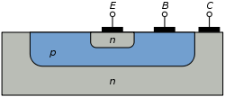
A diffusion transistor is a bipolar junction transistor (BJT) formed by diffusing dopants into a semiconductor substrate. The diffusion process was developed later than the alloy junction and grown junction processes for making BJTs.
Bell Labs developed the first prototype diffusion transistors in 1954.[1]
Diffused-base transistor
The earliest diffusion transistors were diffused-base transistors. These transistors still had alloy emitters and sometimes alloy collectors like the earlier alloy-junction transistors. Only the base was diffused into the substrate. Sometimes the substrate formed the collector, but in transistors like Philco's micro-alloy diffused transistors the substrate was the bulk of the base.
Double diffusion
At Bell Labs Calvin Souther Fuller produced basic physical understanding of a means of directly forming the emitter, base, and collector by double diffusion. The method was summarized in a history of science at Bell:[2]
- "Fuller had shown that acceptors of low atomic weight diffuse more rapidly than donors, which made possible n–p–n structures by simultaneous diffusion of donors and acceptors of appropriately different surface concentrations. The first n layer (the emitter) was formed because of the greater surface concentration of the donor (for example, antimony). The base formed beyond it because of the more rapid diffusion of the acceptor (for example, aluminum). The inner (collector) boundary of the base appeared where the diffused aluminum no longer over-compensated the n-type background doping of the original silicon. The base layers of the resulting transistors were 4 μm thick. ... Resulting transistors had a cut-off frequency of 120 MHz."
Mesa transistor
Texas Instruments made the first grown-junction silicon transistors in 1954.[3] The diffused silicon mesa transistor was developed at Bell Labs in 1955 and made commercially available by Fairchild Semiconductor in 1958.[4]
These transistors were the first to have both diffused bases and diffused emitters. Unfortunately, like all earlier transistors, the edge of the collector–base junction was exposed, making it sensitive to leakage through surface contaminats, thus requiring hermetic seals or passivation to prevent degradation of the transistor's characteristics over time.[5]
Planar transistor

The planar transistor was developed by Dr. Jean Hoerni[6] at Fairchild Semiconductor in 1959. The planar process used to make these transistors made mass-produced monolithic integrated circuits possible.
These transistors have a silica passivation layer to protect the junction edges from contamination, making inexpensive plastic packaging possible without risking degradation of the transistor's characteristics over time.
The first planar transistors had much worse characteristics than alloy junction transistors of the period, but as they could be mass-produced and alloy junction transistors could not, they cost much less and the characteristics of planar transistors improved very rapidly, quickly exceeding those of all earlier transistors and making earlier transistors obsolete.
References
- ↑ Transistor Museum, Historic Transistor Photo Gallery, Bell Labs Prototype Diffused Base Triode
- ↑ Millman (1983) p 426
- ↑ Lécuyer, Christophe; Brock, David C. (2010). Makers of the Microchip: A Documentary History of Fairchild Semiconductor. MIT Press. ISBN 9780262014243., p. 11.
- ↑ Lécuyer & Brock 2010, pp. 10–22
- ↑ Riordan, Michael (December 2007). "The Silicon Dioxide Solution: How physicist Jean Hoerni built the bridge from the transistor to the integrated circuit". IEEE Spectrum. IEEE. Retrieved November 28, 2012.
- ↑ Transistor Museum, Historic Transistor Photo Gallery, Fairchild 2N1613
- S. Millman editor (1983) A History of Engineering and Science in the Bell System, volume 4: Physical Sciences, Bell Labs ISBN 0-932764-03-7 .
- F.M. Smits editor (1985) A History of Engineering and Science in the Bell System, volume 6: Electronics Technology, pp 43–57, Bell Labs, ISBN 0-932764-07-X .