Lattice delay network
Lattice delay networks are an important subgroup of lattice networks. They are all-pass filters, so they have a flat amplitude response, but a phase response which varies linearly (or almost linearly) with frequency. All lattice circuits, regardless of their complexity, are based on the schematic shown below, which contains two series impedances, Za, and two shunt impedances, Zb. Although there is duplication of impedances in this arrangement, it offers great flexibility to the circuit designer so that, in addition to its use as delay network (as featured here) it can be configured to be a phase corrector,[1] a dispersive network,[2] an amplitude equalizer,[3] or a low pass (or bandpass) filter,[4] according to the choice of components for the lattice elements .
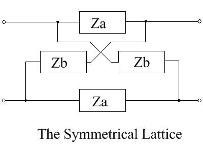
It is shown in Lattice networks that when a lattice is configured as a delay network, it has a characteristic impedance which is resistive (= Ro), its impedances Za and Zb are dual impedances, i.e. Za·Zb = Ro2 (or Za/Ro = Ro/Zb) and Za and Zb consist of inductors and capacitors. Such a lattice is a constant resistance network and an all-pass filter, and it has a phase response determined by the properties of Za. This makes it ideal as a delay device because it can be included in a cascade of other filter sections without affecting the overall amplitude response, nor will it create mismatch problems, but it will increase the phase slope (i.e. the delay) of the overall assembly.
In order to achieve a desired delay, it is necessary to choose specific components for Za and Zb, and the design methods to do this are given in later sections. However, regardless of the method used, networks only achieve a constant delay over a finite band of frequencies, so if an increase in bandwidth and/or delay is required, more complex solutions for Za and Zb are necessary.
Normally Za and Zb are lumped element impedances, suitable for networks operating at audio or video frequencies but operation up to v.h.f. and even u.h.f. is also possible. Sometimes, the design procedures can result in Za and Zb being highly complicated networks, but it is always possible to derive a cascade of simpler lattices with identical electrical characteristics,[4] should that be preferred.
A lattice delay section has twice the delay of a comparable ladder filter section, and this helps to mitigate concerns over component duplication. In any case, a lattice configuration can be converted to an unbalanced equivalent, which will reduce the component count and permit some relaxation of component tolerances.[5] Consequently, lattice delay sections, or their bridged T circuit equivalents, are able to provide substantial time delays in a compact physical form and they make efficient use of their operational bandwidth. Although there are other ways of achieving signal delays, such as by a long length of coaxial cable, or by lumped element ladder networks, such solutions have either greater physical bulk, or they make inefficient use of a frequency band, or they have poor phase linearity.
Design methods for lattice delays
Initially, the designs for lattice delays were based on image theory[4][6] in which the aim was to simulate a finite length of transmission line. Later, network synthesis methods were introduced.
A commonly chosen response for the delay network is the maximally flat group delay characteristic.[7] This delay response is ripple free and is perfectly smooth over the passband, only deviating from the mean value as the band edge is reached. Initially, such a response might be thought to be ideal for a delay network, but it is not necessarily the most efficient and in order to achieve a wider bandwidth, for a given delay, a higher order network is required. However, some increase in bandwidth is also possible, without increasing circuit complexity, by considering alternative characteristics, where the phase and group delay responses are allowed to ripple within the passband[8]’.[9]
There are several design procedures available by which a desired linear-phase approximation can be achieved, whether maximally-flat or with ripple. These methods include techniques from image theory, by the Potential Analog method, and by a Taylor expansion of a group delay, all of which are described in the following sections.
In situations where a balanced network is not appropriate, a single ended circuit operating with a ground plane is required. In such cases, the conversion of a lattice into a bridged T circuit is carried out, as described in the article Lattice network. The resulting unbalanced network has the same electrical characteristics as the balanced lattice network on which it is based. An example of this procedure is given in a later section.
Networks derived from image theory
An ideal delay line characteristic has constant attenuation and linear phase variation, with frequency, i.e. it can be expressed by
where τ is the required delay.
As shown in lattice networks, the series arms of the lattice, za, are given by
More generally, for lattice circuits having a delay τ secs., with a characteristic impedance Zo, the expressions for Za and Zb are given by[4]

As e−x and tanh(x) are not rational functions, exact solutions for za and zb are not possible, so some form of approximation has to be used.
Continued fraction approximation
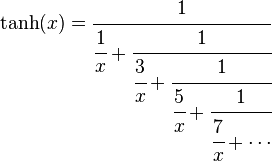
A continued fraction expansion of tanh(x)[1][4][10][11] is
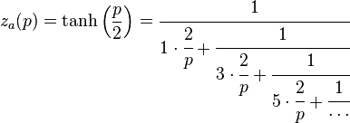
So, for a network with 1sec delay, za can be written
An exact solution requires an infinite number of terms, but an nth order approximation is obtained by terminating za after n elements. (If the last component retained is a capacitor, the remainder of the network is replaced by a short circuit). So, for example, terminating this expression after six terms will give a sixth order delay, which can be synthesised directly by Cauer’s methods[4][11] to give the network shown.
.png)
A circuit for zb can easily found from this solution, since it is the dual of za, and is
.png)
Although this circuit of zb was easy to derive, it is not necessarily the most ideal. If an unbalanced equivalent circuit of the lattice is ultimately required, it would be better if zb started with a series inductor (see Lattice networks). To do this it is first necessary to multiply out the continued fraction expansion for za, for this example, to give za (and zb in particular) as a ratio of polynomials in p. This is
and for the alternative Cauer I expansion proceeds as follows
and so on, until the network shown below is obtained.
.png)
Further details of lattice circuits, using these impedances, are considered in the examples section, later.
Now, as shown in Lattice networks, the transfer function of this lattice is given by
so
From this the phase plot for this sixth-order all-pass function can be calculated and is given below.
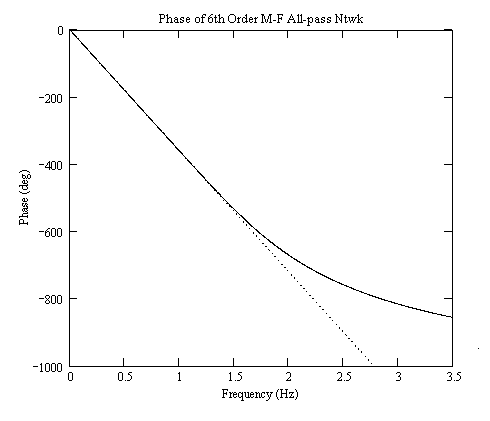
This response is the same as that of the maximally flat delay which is derived in a later section. (In fact, the derivations of za by the continued fraction method result in family of lattices all of which have a maximally flat group delay characteristic). The phase error plot (i.e. the deviation of the response from linear) of this response can be found in the section on maximally flat delay networks, where the responses of networks of several orders are given.
Networks derived using the potential analogue method
The potential analogue method was proposed by Darlington[12] as a simple way to choose pole-zero positions for delay networks. The method allows the designer to implement a delay characteristic by locating poles and zero on the complex frequency plane intuitively, without the need for complicated mathematics or the recourse to reference tables.
Other analogue methods, which were devised to aid the designer to choose the pole zero positions for his networks, include the "rubber sheet model"[13][14] and the "electrolytic tank".[15]
Darlington’s procedure starts by considering the field between the two plates of a parallel plate capacitor. The field is uniform within the plates and only deviates from linear beyond the extremities of the plates. In order to increase the length over which the field is uniform, the length of the plates is increased, as required. The next step is to replace the uniform plates by uniformly spaced charged filaments, which give the same field, but may result in a ‘granularity error’ (or ripple). Finally, the equivalent electrical network is obtained by replacing the localised filament charges by poles and zeros, where the group delay characteristic corresponds to the electric field in the potential analogue.
A typical arrangement of poles and zeros to give, nominally, an electrical circuit with constant group delay follows the pattern shown in the figure below (see also Stewart[1]). The poles and zeros lie in two lines, of finite length, parallel to the jω axis at a distance ‘a’ from it. Also, they are spaced apart at a distance ‘b’ from each other in the jω direction.
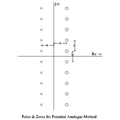
In general, Darlington showed that the group delay and the granularity effect are given by
A good approximation to a unit delay characteristic is obtained by putting a = b = 2π (a value which is easily remembered). However, the delay ripple (granularity) that results, when using these values of a and b, is rather high at ±8% and a better choice for a is 4.4 (= 1.4π) which gives a ripple a lower ripple of ±2.5%. The plots shown below, are for networks with increasing numbers of poles and zeros, for a = 4.4 and b = 2π. The order ‘n’ corresponds to the number of pole-zero pairs present in the network.
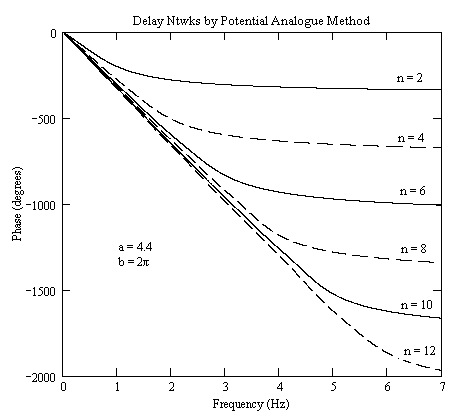
For frequencies beyond the end of the pole zero pattern, the group delay suffers a truncation error, but the band edge performance of a characteristic can be improved, by repositioning the outer poles and zeros slightly, to compensate for this sudden termination of the pattern. Darlington discusses this in his article.[12]
The networks can be realised as a cascade of second order lattices (or their bridged-T equivalents) by allocating a complex conjugate quad of poles and zeros to each section of the cascade (as outlined in Lattice networks). The current example does not have a pole-zero pair located on the real axis, so a first order network is not required.
Networks with a maximally flat group delay characteristic
The general expression for the transfer function of a low pass filter network is given by
The group delay characteristic for this expression can be derived as a power series expansion in ω about zero frequency (i.e. a MacLaurin series). This is described as a maximally flat characteristic when as many as possible of the coefficients of ω in the power series equate to zero, by appropriate choice of values for a, b, c, d, etc.[7][16][17] In deriving this characteristic, little regard is paid to the resulting amplitude response of the low pass filter. (In fact, it approximates to a Gaussian shape).
The time delay for a low-pass network, of order n, with the required characteristics to be maximally flat is given by
where the first (n-1) coefficients of the denominator equal to the corresponding coefficients of the numerator. In this case, when the MacLaurin series for td is derived, by dividing the denominator into the numerator, the result is:
with the first (n − 1) derivatives of td (considered as a function of ω2) at ω = 0 all equal to zero. In this particular expression, the maximally flat response is of order n.
With the maximally flat characteristic, the delay remains constant, equal to the zero-frequency value, over a finite range of frequencies, but beyond this range the delay decreases smoothly with increasing frequency. Higher order networks have a wider bandwidth.
All-pass networks are obtained when zeros are introduced into the right hand half of the complex frequency plane, at locations which are the mirror images of the left hand poles. Such a procedure solves the problem of poor passband responses of the low pass filters, with the added bonus that the resulting networks have the constant resistance property. The general response for the all-pass circuit with maximally flat delay is given by

Introducing zeros, in this way, gives double the delay of an all-pole low pass filter, but the phase characteristic still retains the desired maximally flat feature. The circuit can be realized as a single lattice network, or a cascade of low order lattices, as shown later in some examples, as in lattice networks.
As an example of how a typical derivation proceeds, consider a 6th order low pass filter function. Its transfer function T(p) is given by
The aim is to determine values for a, b, c, d, e, and f so that the group delay of the function is maximally flat.
And the phase response of the function is φ, where
where
and
The group delay is
Inserting the expressions for u and v and rearranging gives the following equation for group delay. Note that the group delay is by doubled, at this point, so that the results will apply to a sixth order all-pass network, rather than for the low-pass network. Thus we have
By choosing GD = 1 when ω = 0 and equating coefficients in the numerator and denominator, six relationships for the six unknowns a, b, c, d, e, and f are obtained, which are:
Solving these six equations for the unknowns gives
So the sixth order all-pass filter with maximally flat delay of 1 sec. is
This expression for T(p) is identical to the one derived earlier, for a sixth order delay, by the continued fraction method.
A similar procedure can be used to determine the transfer functions of networks of all orders, that have a maximally flat time delay, although the procedure does become tedious for the higher orders. A more convenient way of deriving the coefficients of the polynomials is to note that they are based on Bessel polynomials, and the coefficients for all-pass networks are given by[18][19]
Alternatively, the values can be obtained by inspection of published tables.[7][16][17][20][21] Note, however, that the results in most of these tables are for normalised low-pass networks (all-pole networks) of 1 second delay, so using the given coefficient values directly in an all-pass expression will result in a circuit with a delay of 2 seconds.
A selection of results, for even order all-pass networks with n = 2 to 12 are given below. For brevity, the polynomials are not given in full, only the coefficients are listed.
For these results, consider T(p) to have the form 
In the denominator polynomial D(p), all coefficients are positive, whereas in the numerator polynomial N(p), the negative values are taken for the coefficients, whenever indicated.
n = 2 1; ±6 12
n = 4 1; ±20; 180; ±840; 1680
n = 6 1; ±42; 840; ±10080; 75600; ±332640; 665280
n = 8 1; ±72; 2520; ±55440; 831600; ±8648640; 60540480; ±259459200; 518918400
n = 10 1; ±110; 5940; ±20592; 504504; ±90810720; 1210809600; ±11762150400; 79394515200 ±335221286400 670442572800
n = 12 1; ±156; 12012; ±600600; 21621600; ±588107520; 12350257920; ±2001132771840; 2514159648000 ±23465490048000; 154872234316800; ±647647525324800; 1295295050649600
The pole and zero locations in the complex frequency plane for these responses, obtained by factorization of the polynomials, are as follows.
n = 2 ±3.0 ±j1.7321
n = 4 ±5.7924 ±j1.7345 ±4.2076 ±j5.2548
n = 6 ±8.4967 ±j1.7350 ±7.4714 ±j5.2525 ±5.0319 ±j8.9854
n = 8 ±11.1758 ±j1.7352 ±10.4097 ±j5.2324 ±8.7366 ±j8.8289 ±5.6780 ±j12.7078
n = 10 ±13.8441 ±j1.7353 ±13.2306 ±j5.2231 ±11.9351 ±j8.770 ±9.77244 ±j12.4500 ±6.2178 ±j16.4654
n = 12 ±16.4864 ±j1.8777 ±16.0337 ±j5.1567 ±14.9063 ±j8.7335 ±13.2282 ±j12.3580 ±10.6595 ±j16.1017 ±6.6859 ±j20.2489
The phase error plots (i.e. the deviation of the phase response from linear) for even order networks from n = 2 to 12 are given in the accompanying figure.
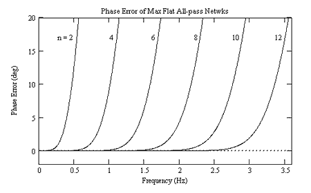
All of the delay characteristics can be realized as a single lattice network, or as a cascade of second-order lattices by allocating a symmetrical group (quad) of two poles and two zeros to each second-order lattice in the network, and using the relationships given in Lattice network. See ‘Examples of lattice circuits’, below, for more information on circuit realization.
Delay networks with passband phase ripple
The maximally flat response is not very efficient. It has an excellent linear phase characteristic within its operating passband, but large complex networks are needed to obtain large delays. However, by allowing the phase response to ripple within the passband, a network of a specific order can achieve a wider bandwidth, (or more delay for a given bandwidth).
The permitted level of delay ripple (or phase ripple) introduced by a circuit is very much dependent on the application in which the network is being used.[22] In situations where waveform or pulse fidelity is important, then the permitted ripple is only small. In the case of analogue television waveforms, for example, the picture content also has a bearing on the acceptable levels of system distortion. (With TV pictures, phase ripple will give effects similar to ‘ghosting’ or multipath reception, where low level multiple images are superimposed on the main picture. Also ‘ringing’ after transient edges is another result of non-linear phase. The acceptability of the picture impairment often depends on the scene being displayed). Wheeler, using the method of "paired echoes", suggested that a phase ripple of 0.1 rads, p-p (or 6 degrees, p-p) was tolerable in TV signals.[23] Other writers suggest that a group delay ripple of a few percent is permissible.[24] In making a judgement of permitted distortion, limits can be set on waveform asymmetry, the level of overshoots and pre-shoots, and rise-time degradation and this is discussed in the section on ‘Transient Testing’ later.
Delay networks derived with a Chebyshev ripple
Details of pole positions for low pass networks that have group delay with a "Chebyshev ripple" characteristic across the passband, for various orders of filter and various levels of ripple have been calculated and published by Ulbrich et al.[8] and by MacNee.[25] The tables below, based on this data, are for all-pass networks. A filter of given order can achieve more delay and/or bandwidth if more passband phase ripple is permitted.
Pole-zero position for all-pass networks with unit mean delay and 1% group delay ripple:
n = 2 ±2.759 ±j1.959
n = 4 ±3.902 ±j2.300 ±3.118 ±j6.698
n = 6 ±4.424 ±j2.539 ±4.176 ±j7.500 ±3.260 ±j12.092
n = 8 ±4.690 ±j2.681 ±4.588 ±j7.985 ±4.285 ±j13.089 ±3.324 ±j17.772
n = 10 ±4.667 ±j2.693 ±4.618 ±j8.049 ±4.493 ±j13.303 ±4.185 ±j18.432 ±3.245 ±j22.931
Pole-zero position for all-pass networks with unit mean delay and 2% group delay ripple:
n = 2 ±2.619 ±j1.958
n = 4 ±3.635 ±j2.380 ±2.958 ±j6.909
n = 6 ±3.965 ±j2.620 ±3.778 ±j7.741 ±3.029 ±j12.466
n = 8 ±4.204 ±j2.739 ±4.127 ±j8.164 ±3.895 ±j13.398 ±3.099 ±j18.189
n = 10 ±4.213 ±j2.829 ±4.178 ±j8.459 ±4.086 ±j13.997 ±3.854 ±j19.319 ±3.078 ±j24.176
Pole-zero position for all-pass networks with unit mean delay and 5% group delay ripple:
n = 2 ±2.427 ±j2.087
n = 4 ±3.090 ±j2.525 ±2.615 ±j7.308
n = 6 ±3.248 ±j2.731 ±3.141 ±j8.095 ±2.640 ±j13.042
n = 8 ±4.690 ±j2.681 ±4.588 ±j7.985 ±4.285 ±j13.089 ±3.324 ±j17.772
Pole-zero position for all-pass networks with unit mean delay and 10% group delay ripple:
n = 2 ±2.187 ±j2.222
n = 4 ±2.459 ±j2.739 ±2.195 ±j7.730
A delay network can be conveniently made up of a cascade of second order lattice networks, allocating a quad of poles and zeros, from the tables above, to each section. An example of a fourth order network, with 10% group delay ripple is considered later.
Delay ripple by using infinite product approximations
An alternative form of group delay ripple, preferable to the equal amplitude Chebyshev ripple, has low amplitude ripples at low frequencies but ripples of increasing amplitude as frequency increases. This characteristic is more desirable than the Chebyshev one because the phase errors are small at low frequencies, (where the spectrum of a typical waveforms has high energy content) but can be high at higher frequencies (where the energy content of the spectrum is lower).
A suitable ripple characteristic is obtained by taking power series approximations of sinh(x) and cosh(x),[1][10] rather than deriving the continued fraction expansion of tanh(x), as was done earlier. Typically, with this procedure, the ripple on the phase characteristic deviates by ±5% from the mean (linear) value.
These results are similar to those obtained by the ‘Forced Ripple Method’,[9][26] where a technique of curve fitting, at a finite number of frequencies of the phase response, is employed.
For normalized networks (Zo = 1) with unit time delay, the equations for za and zb can be written
sinh(x) and cosh(x) can be represented by infinite products,[1][10] and these are
So, for a unit delay network
Terminating the series after a finite number of terms gives a limited bandwidth approximation for 1sec delay. So, for example, an expression to including terms up to p4 will give a fourth order delay network. In this case, za is
which can be realized as a ladder network using Cauer’s procedure,[4] to give the circuit below for za. As before, the dual network, zb, is easily obtained by inspection.
.png)
As already stated, the transfer function of a normalized lattice all-pass network is given by
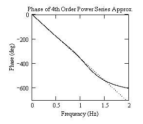
so for the fourth order network containing the impedance za,derived by the power series expansions, is
This has an all-pass magnitude characteristic, with the phase response shown in the figure below.
A collection of results, for even order networks with n = 2 to 10 are given below. (As with results given earlier, the polynomials are not presented in full, only the coefficients are listed).
In these results,  where the coefficients for the numerator and denominator polynomials are listed. For the denominator, D(p), all coefficients are positive, whereas for the numerator, N(p), the negative values are taken where indicated.
n = 2 1; ±K2; π2 where K2 = π2/2
n = 4 1; ±K4; 80π2; ±4π2.K4; 9π4 where K4 = 1×9π2/2×4 = 9π2/8
n = 6 1; ±K6; 35π2; ±20π2.K6; 259π4; ±64π2.K6; 225π6 where K6 = 1×9×25×π2/2×4×16 = 225π2/128
n = 8 1; ±K8; 84π2; ±56π2.K8; 1974π4; ±784π4.K8; 12916π6; ±2304π6.K8; 11025π8 where K8 = 1×9×25×49π2/2×4×16×36 = 11025π2/4608
n = 10 1; ±K10; 165π2; ±120π2.K10; 8778π4; ±4368π4.K10; 172810π6 ; ±52480π6.K10; 1057221π8; ±147456π8.K10; 893025π10 where K10 = 1×9×25×49×81π2/2×4×16×36×64 = 893025π2/294912
The pole and zero locations in the complex frequency plane, for these responses, are as follows.
n = 2 ±2.4674 ±j1.9446
n = 4 ±2.08573 ±j6.999720 ±3.46592 ±j2.10266
n = 6 ±1.65372 ±j12.92985 ±2.95253 ±j7.141180 ±4.06821 ±j2.18380
n = 8 ±1.39164 ±j19.08424 ±2.39805 ±j13.00016 ±3.51463 ±j7.234452 ±4.50223 ±j2.23670
n = 10 ±1.22048 ±j25.3044 ±2.03964 ±j19.12346 ±2.90618 ±j13.05263 ±3.93447 ±j7.30403 ±4.84234 ±j2.27510
The phase error responses for the even order networks from n = 2 to n = 10 have been plotted in the accompanying figure.
.png)
Comparing the bandwidths of networks with passband ripple to those with a maximally flat response, an increase of approximately 50% is achieved.
Comparing three networks
As an example, consider the performance of a sixth order maximally flat delay network with two fourth order networks, one with Chebyshev ripple, and one using the power series approximation. The figure below compares the phase error plots of these three networks (the full line is for the maximally flat response, the dot-dash line for the Chebyshev response and the dashed line for the power series approximation).
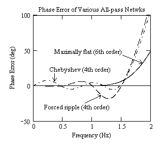
As can be seen, all three normalised delay networks have a nominal linear phase bandwidth of 1.6 Hz (10 rads/s).
In order to compare the performance of the 4th order networks with the maximally flat circuit, it is necessary to use appropriate test waveforms. For example, in the case of television signals, sine-squared pulses may be used for the purpose[27][28]
Some examples of lattice delay circuits
All networks given below are normalized for unit delay and one ohm terminations. To scale for a delay of τ secs., multiply all C and L values by τ. To scale for a different impedance level Ro, multiply all L values by Ro and divide all C values by Ro.
Circuits for a sixth order maximally flat response
Circuits having a single lattice
The first example gives the circuit for a 6th order maximally flat delay. Circuit values for za and zb for a normalized lattice (with zb the dual of za) were given earlier. However, in this example the alternative version of zb is used, so that an unbalanced alternative can be easily produced. The circuit is
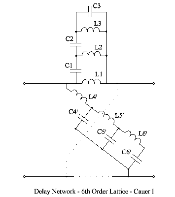
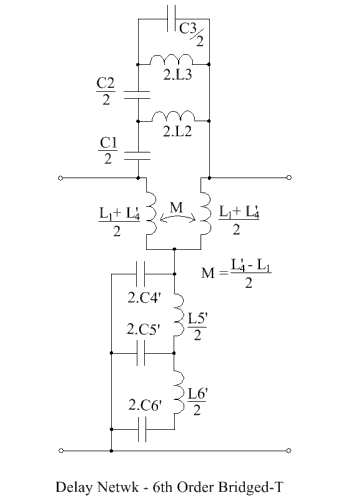
where component values for a normalised 1 ohm network, with 1 second delay at low frequencies, are:
L1 = ½ = 0.5 C1 = 1/6 = 0.16667 L2 = 1/10 = 0.1
C2 = 1/14 = 0.07143 L3 = 1/19 = 0.05556 C3 = 1/22 = 0.04545
and
L4' = 0.02381 C4' = 0.070 L5' = 0.11231
C5' = 0.15027 L6' = 0.19104 C6' = 0.2797
Using the procedures of Lattice networks, this can be converted to an unbalanced form, to give
Circuits with a cascade of low-order lattices
It is often desirable to decompose a lattice into a cascade of lower order networks, because component tolerances can be relaxed.
To carry out the procedure take the three sets of pole-zero data from the table for maximally flat functions, for n = 6, and use the methods in Lattice networks
xA = 8.4967 yA = 1.7350 xB = 7.4714 yB = 5.2525 xC = 5.0319 yC = 8.9854
So for lattice A
C1A = 1/2.xA = 0.05885 = L2A and L1A = 2.xA/(xA2 + yA2) = 0.2260 = C2A
For lattice B
C1B = 1/2.xB = 0.06692 = L2B and L1B = 2.xB/(xB2 + yB2) = 0.1791 = C2B
For lattice C
C1C = 1/2.xC = 0.09937 = L2C and L1C = 2.xC/(xC2 + yC2) = 0.09489 = C2C
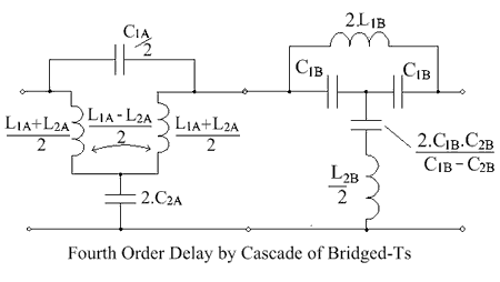
These component values are used in the circuit shown below.
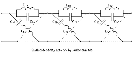
The phase characteristic of this three section cascade is, of course, identical to that of the single complex lattice, given earlier.
This cascade of second order lattices can be converted to an unbalanced configuration by the methods of Lattice networks, and the resulting circuit is shown.
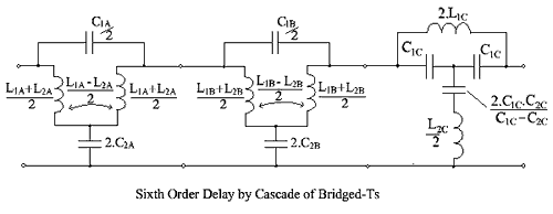
Circuits with phase ripple
Chebyshev, 4th order with 10% GD ripple
From the tables of Chebyshev data, given above, find the pole-zero positions:
xA = 2.459 yA = 2.739 xB = 2.195 yB = 7.730
So for lattice A
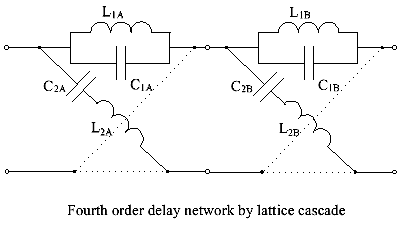
C1A = 1/2.xA = 0.2033 = L2A and L1A = 2.xA/(xA2 + yA2) = 0.3630 = C2A
For lattice B
C1B = 1/2.xB = 0.2280 = L2B and L1B = 2.xB/(xB2 + yB2) = 0.06799 = C2
So use these values in the circuit below.
Circuit for the 4th-order forced ripple approximation
From the tables for power product approximation, given above, find the pole-zero positions:
xA = 3.4659 yA = 2.1027 xB = 2.0857 yB = 6.9997
So for lattice A
C1A = 1/2.xA = 0.1443 = L2A and L1A = 2.xA/(xA2 + yA2) = 0.4218 = C2A
For lattice B
C1B = 1/2.xB = 0.2397 = L2B and L1B = 2.xB/(xB2 + yB2) = 0.07820 = C2B
Use these values in the circuit shown above.
Both 4th order networks can be converted to unbalanced form using the procedures of Lattice networks
See also
References
- 1 2 3 4 5 Stewart J.L., "Fundamentals of Signal Theory", McGraw Hill, 1960
- ↑ Cook C.E. and Bernfeld M., "Radar Signals", Artech House MA, 1993, ISBN 0-89006-733-3, (p.413)
- ↑ Rounds P.W. and Lakin G.L., "Equalization of Cables for Local Television Transmission", BSTJ, July 1955 (pp. 713–738)
- 1 2 3 4 5 6 7 Guillemin E.A., Communication Networks, Vol II", Wiley N.Y., 1935
- ↑ Bode H.W. , "Network Analysis and Feedback Amplifier Design", Van Nostrand, N.Y., 1945
- ↑ Hebb M.H., Horton C.W. and Jones F.B., "On the Design of Networks for Constant Time Delay – image theory content", Jour of Applied Physics, Vol. 20, June 1949
- 1 2 3 Thomson W.E., "Networks with Maximally-Flat Delay", Wireless Engineer, October, 1952, (pp. 256–262).
- 1 2 Ulbrich E. and Piloty H., "Uber den Entwirf von Allpassen, Tiefpassen und Bandpassen mit einer im Tschebyscheffschen Sinne approximierten konstanten Gruppenlaufzeit", Arch. Eleckt. Ubertragung, Vol. 14, Oct. 1960, (pp. 457–467)
- 1 2 Dewsnap G.D., The Approximation of a Time Delay", Proc. IRE (Australia), Vol.25, March 1964 (pp. 168–174)
- 1 2 3 Abramowitz M. and Stegun I.A., "Handbook of mathematical functions", Nat. Bur. Standards 1964, reprinted by Dover Publications N.Y., 1965 (9th ed. 1972),(p.85)
- 1 2 Weinberg L., "Network Analysis and Synthesis", McGraw-Hill, 1962 (p.193)
- 1 2 Darlington S., "The Potential Analogue Method of Network Synthesis", BSTJ, April 1951, (pp. 315–364)
- ↑ Bradley W.E., "Wideband Amplification – the Elastic Sheet Model", Chapter 12 of Television Engineering Handbook, ed. D.G. Fink, McGraw-Hill, 1957.
- ↑ Pramanik A., "Electromagnetism Volume 1(Theory)", Chapter 5, PHI Learning Private Ltd., New Delhi, 2014.
- ↑ Edwards R., Demetrio, T., and Johnson, D., "Resurrecting the Electrolytic Plotting Tank," Proceedings, American Society for Engineering Education Annual Conference and Exposition, AC 2011–1819, Vancouver, BC, June 2011
- 1 2 Thomson W.E., "Delay Networks having Maximally-Flat Frequency Characteristics", Proc. IEE, Vol.96, Part III, (pp. 487–490)
- 1 2 Stewart J.L., "Circuit Theory and Design", McGraw Hill, 1956 (pp. 166–167)
- ↑ Storch L., "Synthesis of Constant-Time-Delay Ladder Networks Using Bessel Polynomials", Proc. IRE, Nov 1954 (pp.1666-1675
- ↑ Henderson K.W. and Kautz W.H., "Transient Responses of Conventional Filters", IRE Trans on Circuit Theory, Vol. CT-5, Dec.1958, (pp. 333–347))
- ↑ Weinberg L., Additional Tables for Design of Optimum Ladder Networks", Journal of the Franklin Institute, August 1957, Section IV Maximally Flat Time Delay, (pp. 127-138)
- ↑ Weinberg L., "Network Analysis and Synthesis", McGraw-Hill, N.Y., 1962
- ↑ Neirynck J.J., "Transient behaviour of systems with equal-ripple delay", IEEE Trans. on Circuit Theory, CT-11, June 1964, (pp.202-3)
- ↑ Wheeler H.A., "The Interpretation of Amplitude and Phase Distortion in Terms of Paired Echoes", Proc. IRE, June 1939 (pp. 359–385)
- ↑ Uberte T.A., "Transient Behaviour of Systems with Equal-Ripple Delay", IEEE Trans. on Circuit Theory, Vol. 11, Issue 2, Jan 1964, (pp. 302–3).
- ↑ MacNee A. B., "Chebyshev Approximation of a Constant Group Delay", IEEE Trans on Circuit Theory, June 1963, (pp.284-285)
- ↑ Valand J., "On the Linear Phase Approximation", Proc. IEEE, Proc. Letters, Sept. 1967 –(more general than Dewsnap) (pp. 1627–1628)
- ↑ MacDiarmid I.F., "A Testing Pulse for Television Links", Proc. IEE Part III, Vol 99, 1952 (pp. 436–444).
- ↑ MacDiamid I.F. & Phillips B., "A Pulse and Bar Waveform Generator for Testing Television Links", Proc IEE, Vol.105, Part B, (p.440)




![\phi = \arg(t) = \arctan \left[ \frac{\omega (e - c\omega^2 + a\omega^4)}{f - d\omega^2 + b\omega^4 - \omega^6} \right ]](../I/m/1da3974177ea8af5f951f38f34727854.png)


![\sinh(x) = x\prod_{k=1}^ \infty \left ( 1 + \frac{x^2}{k^2 \pi^2} \right ) \qquad \text{and} \qquad \cosh(x) = \prod_{k=1}^\infty \left [ 1+ \frac{4.x^2}{(2k - 1)^2 \pi^2} \right ]](../I/m/c72b7d7ad2b3a2d95f3f05b43c8d0314.png)


