Perfboard

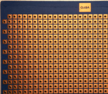
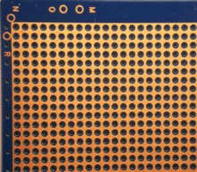
Perfboard is a material for prototyping electronic circuits (also called DOT PCB). It is a thin, rigid sheet with holes pre-drilled at standard intervals across a grid, usually a square grid of 2.54 mm (0.1 in) spacing. These holes are ringed by round or square copper pads. Inexpensive perfboard may have pads on only one side of the board, while better quality perfboard can have pads on both sides (plate-through holes). Since each pad is electrically isolated, the builder makes all connections with either wire wrap or miniature point to point wiring techniques. Discrete components are soldered to the prototype board such as resistors, capacitors, and integrated circuits. The substrate is typically made of paper laminated with phenolic resin (such as FR-2) or a fiberglass-reinforced epoxy laminate (FR-4).
The 0.1 in grid system accommodates integrated circuits in DIP packages and many other types of through-hole components. Perfboard is not designed for prototyping surface mount devices.
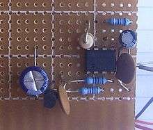
Before building a circuit on perfboard, the locations of the components and connections are typically planned in detail on paper or with software tools. Small scale prototypes, however, are often built ad hoc, using an oversized perfboard.
Software for PCB layout can often be used to generate perfboard layouts as well. In this case, the designer positions the components so all leads fall on intersections of a 0.1 in grid. When routing the connections more than 2 copper layers can be used, as multiple overlaps are not a problem for insulated wires.
Once the layout is finalized, the components are soldered in their designated locations, paying attention to orientation of polarized parts such as electrolytic capacitors, diodes, and integrated circuits. Next, electrical connections are made as called for in the layout.
One school of thought is to make as many connections as possible without adding extra wire. This is done by bending the existing leads on resistors, capacitors, etc. into position, trimming off extra length, and soldering the lead to make the required electrical connection. Another school of thought refuses to bend the excessive leads of components and use them for wiring, on the ground that this makes removing a component later hard or impossible, e.g. when a repair is needed.
If extra wires need to be used, or are used for principal reasons, they are typically routed entirely on the copper side of perfboards. Because, as opposite to strip boards, nearby holes aren't connected, and the only hole in a pad is already occupied by a component's lead. Wires used range from isolated wires, including verowire (enameled copper wire with a polyurethane insulation supposed to melt when soldered), to bare copper wire, depending on individual preference, and often also on what is currently at hand in the workshop.
For insulated wires thin solid core wire with temperature-resistant insulation such as Kynar or Tefzel is preferred. The wire gauge is typically 24 - 30 AWG. A special stripping tool can be used, incorporating a thin steel blade with a slit that the wire is simply inserted into and then pulled loose, leaving a clean stripped end. This wire was developed initially for circuit assembly by the wire wrap technique but also serves well for miniature point-to-point wiring on perfboard. Bare copper wire is useful when merging a number of connections to form an electrical bus such as the circuit's ground, and when there is enough space to properly route connections, instead of wiring them rats-nest style.
Intentional solder bridges can be used to connect adjacent pads when necessary. Careful hand–eye coordination is needed to avoid causing inadvertent short circuits.
Circuits assembled on perfboard are not necessarily fragile but may be less impact-resistant than printed circuit boards.
Perfboard differs from stripboard in that each pad on perfboard is isolated. Stripboard is made with rows of copper conductors that form default connections, which are broken into isolated segments as required by scraping through the copper. This is similar to the pattern of default connections on a solderless breadboard. However, the absence of default connectivity on perfboard gives the designer more freedom in positioning components and lends itself more readily to software-aided design than stripboard or breadboard.


See also
| Wikimedia Commons has media related to Perfboard. |
- Stripboard (Veroboard)
- Breadboard (Protoboard)